your current location is:Home > TechnologyHomeTechnology
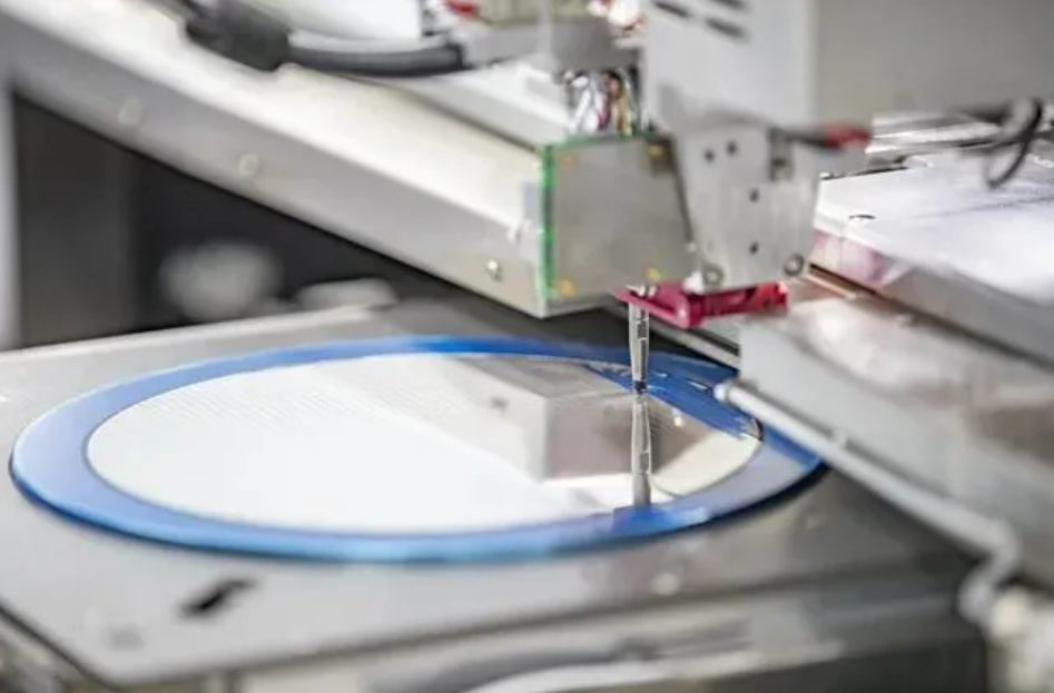
The three giants face off against 2 nanometers: TSMC plans to mass-produce Samsung and Intel in 2025

Our reporter Tan Lun reported in Beijing
Following the first announcement of the 2nm process roadmap in June this year, the high-end process mass production schedule of the closely watched chip manufacturing giant TSMC has also been finalized recently.
According to public reports, TSMC’s advanced process is progressing smoothly. The 3-nanometer will be mass-produced in the second half of this year, the upgraded 3-nanometer process will be mass-produced in 2023, and the 2-nanometer is expected to be mass-produced in 2025.
As the world's most advanced chip process, TSMC 2nm adopts a new architecture for the first time. According to TSMC President Wei Zhejia in a previous technical forum, compared with the 3nm process, the 2nm process chip using the new architecture can increase the frequency by 10% to 15% at the same power consumption, and reduce the power consumption by 25% at the same frequency. to 30%.
It is worth noting that 2nm will be a transition node in terms of TSMC's process. Since the traditional architecture process is close to the performance limit, TSMC's biggest rivals Samsung and Intel have already used the latest process architecture on 3nm, but or out of conservative considerations, TSMC still uses the traditional architecture process for 3nm, which makes TSMC's biggest rivals in the industry. The performance of the 3-nanometer chip has raised a lot of questions.
As the timetable for the latest process has been finalized, the industry believes that TSMC will further widen the gap with Samsung and Intel. Luo Guozhao, director of the China Laboratory of the CHIP Global Testing Center, told the reporter of China Business News that if TSMC's transformation efforts on the 2nm process are successful, it will further magnify its previous advantages in the accumulation of top customers, which also means The Matthew effect in the global chip manufacturing market may further intensify.
Strategic Differences in Architecture Iterations
Although the market prospect of the new architecture is unclear, abandoning the traditional architecture may be only a matter of time for TSMC, which is a leader in the industry, especially under the pressure of Samsung and Intel, the shortcomings of the old architecture are particularly prominent.
For a long time, chip manufacturers have adopted the FinFET (FinFET) architecture in advanced processes. Especially within TSMC, the FinFET technology accumulation is particularly mature, which also helps it continue to lead in the research and development of advanced processes. .
But as chips move into the sub-5nm range, the downsides of FinFETs are starting to emerge. A technical person in charge of a domestic memory chip manufacturer told reporters that there will be leakage effects in the internal transistors when the integrated circuit is powered on. "Traditionally, this effect can be reduced by controlling the spacing of transistors, but when the process reaches a limit, the effect of leakage is inevitable," said the person in charge.
In the industry, this limit node is generally considered to be 3 nanometers. Although TSMC claims to have solved the leakage problem through technical improvements, Samsung, which intends to catch up with TSMC, has made the first change and used a new full-gate field effect crystal ( GAAFET) structure, and announced an early version of 3-nanometer GAA (full-around gate transistor) in 2022, with a "performance version" to ship in 2023.
"The new architecture is not yet very mature, TSMC has always been a steady and steady style, and should not want to be too aggressive in the 3nm strategy. But Samsung is different, they have greatly lagged behind TSMC in 5nm, and they only want to catch up. I can give it a go." Ji Wei, an analyst in the semiconductor industry, told reporters.
Ji Wei said that in fact, TSMC has been carrying out the research and development of GAAFET, and is preparing to switch from FinFET to GAAFET at 2 nanometers, which will be more reasonable in terms of cost transition. In terms of 3 nanometers, TSMC has also upgraded the corresponding FinFET architecture. It still guarantees the stability of product performance.
It is worth noting that Samsung did pay a price for its aggressive process strategy. Due to problems with the yield rate of the new architecture, Samsung announced in mid-2021 that the 3-nanometer chip originally planned to be put into production in 2022 will be postponed for one year to 2023, which is almost the same as TSMC. Therefore, in terms of results, Samsung's preemptive plan did not succeed.
Luo Guozhao believes that for TSMC, which holds orders from many first-tier manufacturers such as Apple, the priority of production line and shipment stability is higher than technological innovation. This stability also means that TSMC will only adopt a new architecture on 2nm if it is fully confident.
Mature process is still the mainstream
Although the high-end manufacturing process is in full swing, for the chip market, mature manufacturing process is still the mainstream market demand.
According to data released by TSMC, even 5G smartphones using the most advanced 5nm process currently have a lot of mature process chips, such as various sensors, audio, radio frequency, power management and other chips. A single mobile phone carries nearly 100 pieces, and most of its main manufacturing processes are below 28 nanometers, and some even reach the micron level.
"The process competition between TSMC and Samsung has attracted too much market attention. In fact, from the perspective of demand, products above 10 nanometers, especially above 28 nanometers, are the products with the highest shipments in the global chip industry." Ji Wei said, this On the one hand, it is determined by the demand, and on the other hand, it is determined by the cost of the high-precision process.
The report of the International Semiconductor Industry Association pointed out that taking a 5-nanometer chip using FinFET process as an example, its design cost is nearly 8 times that of a 28-nanometer process, while the cost of a more complex GAAFET architecture is higher, and this is only a part of the chip design. cost. The actual research and development technology, factory construction, and purchase of production equipment of chip foundries have not been included in the calculation.
"Like many industries, this kind of high-cost game is destined to be only affordable by the leading manufacturers, and most mainstream manufacturers will still focus on the mainstream demand of the market." Luo Guozhao said that taking Intel as an example, its Although the research and development on 7-nanometer has been delayed, apart from stock price fluctuations, revenue and profits have not been affected too much, precisely because its 10-nanometer and above products are the core of its shipments.
Luo Guozhao said that taking the automobile industry with the most serious shortage of cores as an example, the most in short supply of microcontroller chips mainly uses 8-inch wafers, and the chip manufacturing process is generally between 45 and 130 nanometers, which makes the chip market except for giants , the enthusiasm for advanced processes does not invest too much energy.
TrendForce's latest forecast report shows that the global wafer foundry capacity will increase by about 14% annually in 2022, of which the 12-inch annual growth rate will reach a double-digit 18%. About 65% of the new 12-inch capacity is the mature process of 28 nanometers and above, so it is expected that the annual growth rate of the mature process is expected to reach 20%.
The Big Three Battle for 2nm
As the top process enters the 2nm node, the three chip giants TSMC, Samsung and Intel will also usher in a new showdown.
According to public information, the land for the second-phase expansion plan of TSMC’s 2-nanometer factory has been finalized, and it is planned to start construction in the third quarter of this year; Samsung announced in July this year that it has begun preliminary production of 3-nanometer process chips using the GAAFET architecture, while the 2-nanometer GAAFET process The mass production time is also set in 2025; Intel previously promised to regain the leading position in chip manufacturing technology by 2025, and set the time target for 2nm production in 2024.
It's worth noting that Intel also released a timetable for 1.8nm. According to Intel CEO Pat Kissinger, 1.8-nanometer will be launched six months ahead of schedule, that is, the market will be able to see its movement by the end of 2024.
Ji Wei previously told reporters that if Intel can launch the 1.8-nanometer process as scheduled, it will obviously catch up with the research and development progress of TSMC and Samsung, and even change the current competition pattern of "two heroes competing for hegemony". TrendForce data shows that as of the end of 2021, TSMC is the world's largest chip foundry, with a market share of nearly 52.9%, while Samsung ranks second with a market share of 17.3%.
However, for the challenge initiated by Intel, Luo Guozhao believes that the feedback from the chip market often takes a long period of time, and after Intel was previously opened up by TSMC and Samsung in 10nm and 7nm, it also takes a long time to regain the trust of customers. Longer time, so catching up will be a long process. "At least in the current global foundry share, Intel is still behind rivals such as UMC and GlobalFoundries." He said.
More importantly, in Luo Guozhao's view, TSMC's advantage has been established, and this advantage is based on the top process. TSMC's 2021 financial report shows that shipments of 5nm chips account for 20% of its total revenue, and 7nm accounts for 30%. "This means that the advanced process accounts for almost half of TSMC's revenue, and this ratio is terrible." Luo Guozhao said, this means that TSMC's advantage over its rivals in advanced processes is not only difficult to narrow, but may be further enlarged.
In addition, public information shows that TSMC's capital expenditure in the second half of 2022 will increase significantly, and it may exceed US$40 billion next year, of which 3nm wafer foundry from major customers such as Apple, Intel, Supermicro, and Nvidia from 2023 to 2025 Strong demand accounts for the majority.
In this context, TSMC is undoubtedly still firmly grasping the advantages of 2nm. Ji Wei believes that in the foreseeable future, Samsung and Intel will not be able to catch up with TSMC for the time being, and the pattern of one super and two strong in the global chip foundry market may continue.
The reporter contacted TSMC, Samsung, and Intel for interviews on issues related to the nano-fabrication process, but no reply was received as of press time.


related articles
Article Comments (0)
- This article has not received comments yet, hurry up and grab the first frame~
Special recommendation


Random recommendation

-

The controversial "labor dispatch" has actuall...
2022-08-18 13:20:03 -

Musk thinks self-driving cars are the future,...
2022-09-16 14:10:54 -

Why did the Japanese rocket self-destruct aft...
2022-10-13 17:36:01 -

Amazon CEO accused of violating labor laws for obstructing union formation
2022-10-27 18:05:51
Click to rank

-
Apple slams the Android App Store, firmly op...
2018-05-15 20:35:22 -

What did Musk's exposed Twitter document door say?
2022-12-09 12:30:39 -
Billboard announces entry into China and seek...
2022-08-09 13:21:59 -
From suppression to cooperation: the United S...
2022-08-01 11:36:48
Tag Cloud
about us
-
The European Financial Times provides 7X24 hours of global financial information and financial market news, covering stocks, bonds, funds, futures, trusts, wealth management, management and other services for individuals and businesses.